GPU Memory Pools in D3D12
When the monkey’s paw granted our wish for lower-level/explicit graphics APIs, one of the consequences was that we were much more directly exposed to the fact that GPUs can have their own separate set of physical memory. Anybody that’s ever had to purchase a dedicated video card for their PC can probably tell you that such a video card has its own set of physical RAM chips on the board that are reserved for the GPU. Meanwhile, the integrated GPUs often used in laptops and mobile devices will typically share one set of RAM with the CPU. This reality can make things complicated for a graphics programmer, since you potentially have two different physical pools of “GPU memory” that will have different characteristics depending on how you’re using it. Earlier APIs such as D3D11 and OpenGL sort of exposed these pools by abstracting away GPU memory altogether behind different resource types, but in D3D12 and Vulkan you are now more-or-less directly exposed to lower-level allocation and management of GPU memory. Altogether it’s complicated enough to cause confusion and headaches for beginners or even experienced graphics programmers, and it tends to come up rather early since you usually need to grapple with it before you can create your first texture.
In this article we’re going to dive in on this topic, and in particular cover the following things:
- The basics of GPU memory
- How GPU memory works in D3D12
- Common patterns in D3D12
- Some timing results gathered from a D3D12 test app
Ultimately I’m going to cover a lot of things that were already covered in some form by Adam Sawicki’s excellent talk from Digital Dragons 2021 about optimizing for GPU memory pools. I would recommend watching that talk either way, but I’m hoping that this article can complement that presentation by adding some extra details as well as some real-world benchmark results.
To keep this article somewhat focused, I’m also only going to talk about D3D12 here and ignore other APIs. I would suggest reading Adam’s post about Vulkan memory types if you’re looking for information specific to Vulkan. You can also check out his later post about D3D12 memory types and pools for a great overview of how memory pools are exposed through the D3D12 API.
Basics of GPU Memory
As I briefly mentioned in the intro, a particular GPU may or may not have its own physically separate pool of memory to use for storing whatever data it needs to access. In general this sort of “split” memory pool setup is something you see on the discrete GPUs found on video cards, whereas the integrated GPUs that are built onto the same die as the CPU will typically use the same physical memory as the CPU. To start, let’s look at the latter case which is arguably simpler.
Integrated/UMA GPUs
So-called “integrated” GPUs are what you’ll find built into many of the CPU offerings from Intel as well as the APU offerings from AMD, and are called that because the GPU is literally integrated into the same die as the CPU:
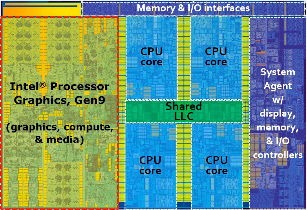
These types of GPU are not a monolith, especially if you look at what you might see in phones, consoles, and Apple/Mac devices. However if you’re looking at the Windows/PC world you can usually assume that the following is true:
- The CPU and the GPU share the same physical memory, and often the same memory controller
- The RAM being used is of the DDR variety typically used for CPUs, as opposed to the more exotic GDDR chips found in video cards
- The amount of raw bandwidth available to the GPU is perhaps an order of magnitude lower than what you might find on high-end dedicated graphics cards. As an example, the Gen12 GPUs found in recent Tiger Lake and Alder Lake CPUs from Intel will range from about ~50 GB/s to ~76 GB/s. Meanwhile an AMD RX 6800 can achieve 512 GB/s to its dedicated Video RAM (VRAM), while an Nvidia RTX 3090 peaks at a whopping 936 GB/s!
Since the CPU and GPU share the same pool of physical memory, this setup is often referred to as a “Unified Memory Architecture”, or UMA for short. While it might seem at first that this is purely a disadvantage relative to a faster dedicated memory pool, this isn’t entirely true. Sharing the memory pool and mechanisms for accessing that memory can make it easier for the CPU and GPU to work together: both processors can directly read and write to the same physical memory addresses, and perhaps even have a shared level of cache hierarchy. This can improve performance for CPU/GPU communication, and also remove certain cases of bugs. The other main advantage is that the system and its applications are free to partition the single pool of memory however they see fit, without having to instead manage two separate pools of memory that can only be used for a single processor.
Dedicated/NUMA GPUs
For a PC that has its own dedicated video card, the situation is of course very different: these video cards have their own bank of physical RAM chips right on the board. Since this RAM pool is physically separate from the CPU RAM, this setup is usually referred to as a “Non-Unifed Memory Architecture” or “NUMA” for short. Often this separate pool is accessed through its own memory controller that’s present on the GPU, and can even have its own separate page tables and virtual address space.
As we mentioned before, dedicated VRAM is capable of achieiving significantly higher bandwidth than what you’ll see for the DDR modules used by PC CPUs. The secret weapon here for VRAM is that they typically use exotic GDDR RAM chips that are specifically designed for high-bandwidth use cases, and these chips are then wired onto very wide 256-bit or even 384-bit buses. The chips, bus, and the GPU itself are all explicitly designed to handle the sort of wide bursts of coalesced memory accesses that you can expect from the 32-wide SIMD arrays that shader programs execute on.
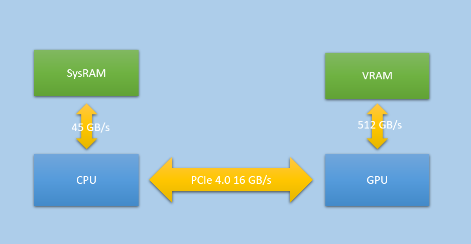
Since the memory pools are physically split on a dedicated GPU setup, sharing data between the CPU and GPU is naturally much more complicated. For sharing to happen, everything needs to happen on the PCI-express bus that the video card is connected to. The GPU is capable of reading from CPU memory (SysRAM) over this bus, which it can do at around 16 GB/s for PCI Express 3.0 and around 32 GB/s with the newer PCI Express 4.0. 16 GB/s really isn’t very much compared with the GPU’s bandwidth to VRAM or even the CPU’s bandwidth to SysRAM, which makes it a resource that has to be utilized rather carefully. A video card will usually have a dedicated DMA unit on board that is optimized for asynchronously “uploading” large chunks of texture or buffer data from SysRAM to VRAM. PCIe can also service general texture and buffer reads issued by the shader core, which can work out well for small buffers that are updated frequently and fit comfortably in caches. The CPU also has the ability to directly write to VRAM over the PCIe bus, through a mechanism known as “Base Address Register”, or BAR for short. Until recently the amount of VRAM accessible through BAR was limited to around 256 MB, limiting its usefulness to special case data that was carefully managed by drivers. More modern systems however can support a feature known as “Resizable BAR”, or ReBAR, which can make the entire pool of VRAM accessible from the CPU.
The fact that the CPU and GPU have their own memory controllers and cache hierarchies can cause further pain and complexity for CPU/GPU communication. PC video cards can typically snoop the caches of the CPU when the CPU writes to GPU-visible SysRAM, however CPU and GPU cache hierarchies are still effectively seperate. This leads to something of a dilemma for the CPU when writing to memory that only the GPU will read from: does it make sense to leave caching enabled and “pollute” the cache with data from GPU, or would it make more sense to bypass the CPU cache entirely? The latter has historically been the default on PC, while making use of a hardware feature known as write combining. This feature effectively buffers nearby writes together so that each individual write doesn’t need its own separate uncached bus transaction, which can work decently as long as you’re doing fairly boring memcpy-style sequential writes. However this does nothing at all for you if you are unlucky enough to try to read from GPU-visible memory: the reads are completely uncached, and they will be quite slow. Things are even worse if you somehow read from VRAM over PCIe, which can be catostrophically slow. Enabling caching can avoid the performance penalty from accidental reads, however it may cause adverse performance for subsequent code by pushing important CPU data out of cache.
How It Works In D3D12
D3D12 applications have to allocate their own memory, so how is all of this exposed to us? Adam Sawicki already gave a great overview of how everything works on his blog, and there is also information in the official programming guide for D3D12. For completeness I’ll provide a brief overview here as well, along with some additional information based on my own experiences.
In D3D12 you have two different ways to allocate GPU-accessible memory for your device: by creating a committed resource, or by creating a heap. Heaps are the more direct way of allocating and utilizing memory, where you must create a heap first with various properties and then “place” resources within that heap via CreatePlacedResource. Committed resources allocate memory indirectly: it’s roughly the same as if the runtime/driver created a single resource-sized heap for you behind the scenes, and then placed the resource in that heap for you. For that reason, we will focus on heaps here instead of committed resources.
Once you’ve created your device, you can query some feature bits in order to get some information in advance about the architecture and behavior of the GPU that you will be allocating memory for. In particular there are two fields of interest on D3D12_FEATURE_DATA_ARCHITECTURE, which you obtain by calling CheckFeatureSupport with D3D12_FEATURE_ARCHITECTURE:
typedef struct D3D12_FEATURE_DATA_ARCHITECTURE
{
    UINT NodeIndex;
    BOOL TileBasedRenderer;
    BOOL UMA;                 // < -- 1
    BOOL CacheCoherentUMA;    // < -- 2
} D3D12_FEATURE_DATA_ARCHITECTURE;
- The
UMAflag tells you if the GPU uses a Unified Memory Architecture where a single physical pool of RAM is shared between the CPU and GPU, like what you’d normally find on an integrated GPU - If
UMAis true andCacheCoherentUMAis also true, then the CPU and GPU caches are fully coherent with each other. In this situation using uncached writes for filling GPU-visible SysRAM does not make sense, since the GPU can benefit from data being resident in cache.
In a bit we’ll talk about how these flags affect the behavior of a device and ways an app can respond to them, but first let’s look at the lowest-level mechanism for creating a heap: creating a “custom” heap. Custom heaps allow the app to fully specify all of the supported attributes of a heap, which is done through these two structs:
typedef struct D3D12_HEAP_DESC
{
    UINT64 SizeInBytes;
    D3D12_HEAP_PROPERTIES Properties;
    UINT64 Alignment;
    D3D12_HEAP_FLAGS Flags;
} D3D12_HEAP_DESC;

typedef struct D3D12_HEAP_PROPERTIES
{
    D3D12_HEAP_TYPE Type;   // Must be D3D12_HEAP_TYPE_CUSTOM
    D3D12_CPU_PAGE_PROPERTY CPUPageProperty;
    D3D12_MEMORY_POOL MemoryPoolPreference;
    UINT CreationNodeMask;
    UINT VisibleNodeMask;
} D3D12_HEAP_PROPERTIES;
First, there is SizeInBytes which is exactly what it sounds like. There is also an Alignment needed for satisfying alignment requirements for specific kinds of resources (in particular, MSAA textures). There is also a set of D3D12_HEAP_FLAGS that you can configure, but they are not generally relevant to our focus on memory pools and so we will ignore this. Instead, let’s look at two of the interesting enums that you can specify in D3D12_HEAP_PROPERTIES:
typedef enum D3D12_MEMORY_POOL
{
    D3D12_MEMORY_POOL_UNKNOWN = 0,  // Not relevant for custom heaps
    D3D12_MEMORY_POOL_L0  = 1,
    D3D12_MEMORY_POOL_L1  = 2
} D3D12_MEMORY_POOL;

typedef enum D3D12_CPU_PAGE_PROPERTY
{
    D3D12_CPU_PAGE_PROPERTY_UNKNOWN = 0,    // Not relevant for custom heaps
    D3D12_CPU_PAGE_PROPERTY_NOT_AVAILABLE = 1,
    D3D12_CPU_PAGE_PROPERTY_WRITE_COMBINE = 2,
    D3D12_CPU_PAGE_PROPERTY_WRITE_BACK  = 3
} D3D12_CPU_PAGE_PROPERTY;
Now things are getting interesting! D3D12_MEMORY_POOL is exactly what it sounds like: it allows us to choose the physical pool of RAM that the memory will live in. On NUMA devices (dedicated video cards) L0 maps to SysRAM AKA CPU memory, while L1 maps to VRAM located on the video card. However on UMA devices there is only physical memory pool available, which is LO. L1 is not available on such devices, and attempting to use it will cause the CreateHeap call to fail. This choice of memory pool must also be carefully paired with an appropriate D3D12_CPU_PAGE_PROPERTY in order to play nice with the CPU’s ability (or lack thereof) to access the memory pool. In practice it ends up working something like this:
if(UMA)
{
    if(MemoryPoolPreference == D3D12_MEMORY_POOL_L0)
    {
        // Memory will live SysRAM pool shared between CPU and GPU
        if(CPUPageProperty == D3D12_CPU_PAGE_PROPERTY_NOT_AVAILABLE)
        {
            // Not accessible to the CPU at all
        }
        else if(CPUPageProperty == D3D12_CPU_PAGE_PROPERTY_WRITE_COMBINE)
        {
            // Uncached for the CPU. Write combined for CPU writes, very very slow CPU reads.
            // Ok for passing data from CPU -> GPU.
        }
        else if(CPUPageProperty == D3D12_CPU_PAGE_PROPERTY_WRITE_BACK)
        {
            if(CacheCoherentUMA)
            {
                // CPU pages are cached, fast for writes and reads.
                // GPU potentially benefits from data being in cache as well.
                // Good for all purposes.
            }
            else
            {
                // Cached for CPU. May not have ideal CPU performance when
                // compared with uncached/write-combined. Good for
                // reading back data from GPU -> CPU
            }
        }
    }
    else if(MemoryPoolPreference == D3D12_MEMORY_POOL_L1)
    {
        // Error, can't use L1 on UMA!
    }
}
else
{
    // NUMA device
    if(MemoryPoolPreference == D3D12_MEMORY_POOL_L0)
    {
        // Memory will live in the SysRAM pool
        if(CPUPageProperty == D3D12_CPU_PAGE_PROPERTY_NOT_AVAILABLE)
        {
            // Lives in SysRAM but the CPU can't access it, don't do this!
        }
        else if(CPUPageProperty == D3D12_CPU_PAGE_PROPERTY_WRITE_COMBINE)
        {
            // Uncached for the CPU. Write combined for CPU writes, very very slow CPU reads.
            // GPU will read this data over PCIe at low speeds relative to VRAM.
            // Good for passing data from CPU -> GPU
        }
        else if(CPUPageProperty == D3D12_CPU_PAGE_PROPERTY_WRITE_BACK)
        {
            // Cached for the CPU with full speed reads and writes.
            // GPU will access this data over PCIe at low speeds relative to VRAM.
            // Good for reading back data from GPU -> CPU.
            // Can be used for CPU -> GPU traffic as well, but may pollute
            // the CPU cache with data that will only be read by the GPU.
        }
    }
    else if(MemoryPoolPreference == D3D12_MEMORY_POOL_L1)
    {
        // Memory will live in the high-bandwidth VRAM pool
        if(CPUPageProperty == D3D12_CPU_PAGE_PROPERTY_NOT_AVAILABLE)
        {
            // The CPU can't access this memory at all, only the GPU can.
            // Good for data that only the GPU will ever read or write, such as render targets.
            // Good for persistent, read-only resources but filling the data requires
            // a two-step upload process.
        }
        else if(CPUPageProperty == D3D12_CPU_PAGE_PROPERTY_WRITE_COMBINE)
        {
            // Error, not valid for a NUMA device
        }
        else if(CPUPageProperty == D3D12_CPU_PAGE_PROPERTY_WRITE_BACK)
        {
            // Error, not valid for a NUMA device
        }
    }
}
This is naturally a bit complicated to manage all of this yourself, so to make things a bit easier D3D12 provides “built-in” heap types that are optimized for common use cases. These types are accessed by using the D3D12_HEAP_TYPE_DEFAULT, D3D12_HEAP_TYPE_UPLOAD, or D3D12_HEAP_TYPE_READBACK values of D3D12_HEAP_TYPE when creating the heap, and setting the MemoryPoolPreference to D3D12_MEMORY_POOL_UNKNOWN and CPUPageProperty to D3D12_CPU_PAGE_PROPERTY_UNKNOWN. Here’s how they work:
DEFAULTis intended for resources that the GPU primarily accesses at full bandwidth. On NUMA this maps to L1 with no CPU access, while on UMA it maps to L0 with no CPU access.UPLOADis intended for CPU -> GPU communication where the CPU writes the data and the GPU reads it. On NUMA this maps to L0 with WRITE_COMBINE CPU access, while on UMA it maps to L0 with WRITE_COMBINE if CacheCoherentUMA is false, and WRITE_BACK if CacheCoherentUMA is true.READBACKis intended for GPU -> CPU communication where the GPU writes the data and the CPU reads it. On both UMA and NUMA devices this maps to L0 with WRITE_BACK CPU access.
One thing you may have noticed about this setup is that CPU-accessible VRAM is not currently exposed through any of these options. While the driver can use the small amount of BAR VRAM if it decides it’s worthwhile, applications have no direct way of allocating from that special bit of memory. This is true even on newer machines with ReBAR support that makes the entire pool of VRAM accessible to the CPU. However, here is an NVAPI extension that allows you to query and allocate from CPU-accessible VRAM if the device was created on a supported Nvidia GPU. Meanwhile, AMD’s driver can automatically promote allocations to CPU-accessible VRAM based on heuristics and ReBAR support. Hopefully a future version of D3D12 adds support for this functionality, since it is certainly a useful option.
It’s not necessarily obvious from reading the official documentation, but these various built-in and custom heap types come with limitations on resource usage that are either implicit or explicit depending on the exact use case. In general buffer resources are not limited: you can place them in any of the built-in heap types as well as any possible configuration of a custom heap, provided that the heap wasn’t created with D3D12_HEAP_FLAG_DENY_BUFFERS. Buffers have an implied linear layout of the data that is similar to an array in C/C++, which makes it trivial for both CPU and GPU to access these resources. Textures however are special: these typically do not use a linear layout1, but instead use a hardware-specific swizzle pattern that’s designed for maximum spatial locality and cache efficiency. This isn’t an issue if the GPU accesses the texture since it knows how to read/write to these special patterns, but it’s a major issue if you wanted to access such a texture from the CPU: your app doesn’t know the swizzle pattern, which means only the driver knows how to encode or decode it. Even if you could access the texture you likely wouldn’t want to read it from SysRAM on a NUMA device, since the slow PCIe bandwidth could degrade performance. The built-in heaps use a heavy-handed means of guarding you from these issues by flat-out forbidding you from creating texture resources in an UPLOAD heap. Instead you must use a “two-step” upload scheme where the CPU writes un-swizzled data to a buffer in UPLOAD memory, and then the GPU itself copies and swizzles the data to a texture resource in DEFAULT memory.
With custom heaps, you can potentially bypass the texture/heap limitations but it must be done carefully. D3D12 will let you place a ROW_MAJOR texture resource in a CPU-writable L0 heap even on a NUMA device, which you can then fill from the CPU. But you should be prepared for excruciatingly poor performance if you try to do this, due poor spatial locality coupled with slow PCIe bandiwdth. A somewhat better option is to use the special WriteToSubresource function, which allows the driver to fill an UNKNOWN-layout texture using a hardware-specific swizzle pattern. This would likely still be too slow on NUMA hardware that reads from L0, however it can be compelling option for UMA devices that share a memory pool anyway. WriteToSubresource allows you to forego a GPU-side copy to initialize your resources, which is appealing since integrated GPUs often lack an asynchronous DMA for performing said copies. WriteToSubresource might one day be relevant for dedicated video cards if ReBAR becomes the norm an D3D12 exposes CPU-accessible VRAM, however it ultimately may not be desirable for apps to burn a CPU core on swizzling texture data.
If you want to keep an eye on how much memory your app is using from the two pools, QueryVideoMemoryInfo can be called from a IDXGIAdapter3 to get the current usage of L0 and L1. To do this you just need to know that DXGI_MEMORY_SEGMENT_GROUP_LOCAL maps to L1, while DXGI_MEMORY_SEGMENT_GROUP_NON_LOCAL maps to L0. The OS-assigned budgets returned by this function are also useful to keep an eye on. In particular if you start to execeed the L1 budget, the OS can start to automatically “demote” some of your heaps from L1 to L0 in order to leave enough free VRAM for other processes on the system. If this demotion happens to the wrong resource it can destroy your performance, and so you really want to avoid that situation if you can help it. PIX for Windows can also show you this information when attached to your app, which is handy. If demotion does occur you can mitigate the damage by assigning a residency priority on your heaps/resources. This can let you keep your more critical resources in VRAM by allowing the OS to demote less-important things.
Common Patterns in D3D12
After discussing some of the specifics of the API, let’s now talk about how D3D12 apps and samples typically work with memory pools.
Textures And The Two-Step Upload
To start, let’s discuss textures since they are somewhat special. As we covered earlier, textures tend to be swizzled in an opaque hardware-specific layout while also being quite large and bandwidth-hungry. Therefore the common choice is to throw these guys in a DEFAULT heap, which maps to the high-bandwidth L1/VRAM pool on NUMA devices (and as we mentioned earlier, the runtime won’t even let you create a texture in an UPLOAD heap). This puts us in our desired physical memory pool on both UMA and NUMA devices, but introduces a separate problem: the CPU cannot directly initialize the contents of a texture living in DEFAULT. Instead we must rely on what I call the two-step upload process, which goes something like this:
- Some memory from a buffer resource living in CPU-accessible memory (typically a UPLOAD heap) needs to be reserved, enough to fit the texture data being uploaded. This is sometimes called a “staging” buffer.
- The CPU loads or copies un-swizzled texture data into the CPU-accessible buffer
- CopyTextureRegion is called on a command list, one for each subresource in the texture (mip level or array slice)
- The command list is submitted on a queue where it executes on the GPU, and proper synchronization is used to ensure tha the copy completes before another command attempts to read from the texture
This process has the GPU effectively accomplish two goals: swizzling the texture data from a linear layout into a hardware-specific texel order, and getting the texture data into fast VRAM. Both are critical for performance, since textures are bandwidth heavy and rely on caching and 2D locality to keep things from slowing down too much. Neither of these are stricly recquired, since it’s possible to allocate textures in SysRAM via custom heaps and you can also specify that a texture resource should use D3D12_TEXTURE_LAYOUT_ROW_MAJOR when creating it. However both of these can come with severe peformance penalties, so it is highly recommended to place textures in VRAM with D3D12_TEXTURE_LAYOUT_UNKNOWN (or D3D12_TEXTURE_LAYOUT_64KB_UNDEFINED_SWIZZLE for tiled resources).
The two-step upload process might sound rather simple at first, but make no mistake: there are many potential paths to take and a lot of subtleties to consider when it comes to allocating staging memory and scheduling the actual copy/upload. We’ll dig into that in a little bit, but first let’s discuss buffers.
Should We Upload Buffers?
The two-step upload is a de-facto requirement for textures, but what about buffers? Unlike textures, buffers can be created in UPLOAD heaps and can be read directly from SysRAM by shaders and copy operations. But wouldn’t they also benefit from being uploaded to VRAM? The answer to that is “yes, sometimes”. For large, read-only or rarely-updated buffers allocating them in VRAM and uploading their contents makes a ton of sense, and you can likely use the same mechanisms that you would use for initializing textures. The situation is slightly easier since you don’t need to worry about CopyTextureRegion and RowPitch alignment requirements, but is otherwise mostly the same.
Things are different though for smaller, frequently-updated buffers. For example, a 64-byte constant buffer containing a per-draw world transform that you update every frame. In these cases the data can fit nicely in cache, so you’re probably not losing very much performance (if any) by letting the GPU read it over PCIe. Also if you’re only reading the constant buffer once, you’re liable to actually make performance worse by copying from SysRAM to VRAM first. Therefore you can usually save yourself the headache for these kinds of small dynamic buffers, and just let them live in SysRAM. If the data is truly fire-and-forget and doesn’t need to persist longer than the current frame being recorded, you can use really fast linear allocator patterns to quickly grab a bit of temporary UPLOAD memory that’s tied to frame lifetime.
Where things get trickier is buffers that are not small, are updated fairly frequently, and are accessed either more than once or with addresses that are unique for every thread of a draw or dispatch. For these cases you probably do want the full bandwidth of VRAM, but uploading their contents every frame can add additional costs and headaches that need to be considered. The simplest option of uploading the data syncronously via a CopyResource or CopyBufferRegion call on the main DIRECT/graphics queue gets the job done, but that introduces additional GPU time on that queue that has to be offset with the improved bandwidth afforded by VRAM. In the next section we’ll talk about more advanced scenarios for uploading data that can potentially result in better overall performance.
Once CPU-accessible VRAM is ubiquitous through ReBAR, it seems plausible that nearly all CPU-updated buffers could live in VRAM and be directly updated from the CPU. This would simplify the situation considerably compared to what’s required now. For integrated UMA GPUs that situation already exists: there’s really no reason to do a two-step upload for buffer resources on these systems, and it would benefit engines to detect this case if they want to optimize for these GPUs.
Working With The COPY Queue
When discussing the two-step upload we mentioned how there are actually many choices and trade-offs to consider when setting up upload paths in your engine. In particular you need to choose how exactly you allocate/aquire the UPLOAD buffer used as the source of the copy, and you also need to decide how and when you submit your command list on a command queue. The official D3D12 samples use a very simple scheme where an UPLOAD buffer is created as a committed resource and the copy is immediately submitted on a DIRECT command queue (via UpdateSubresources from the d3dx12.h helper header) followed by an immediate CPU wait for the submission to finish. That’s totally fine for simple use cases, but what if you have many uploads to do and you don’t want to spend a ton of time creating and destroying committed resources? What if you need to stream in these textures in background while most of your CPU cores are busy and your GPU is already executing giant batches of rendering work on the DIRECT queue? What if there’s a texture or buffer in VRAM that needs to be updated every single frame, and you don’t want updating it to stall out one of your rendering threads? For these situations you probably want a more complex approach that better fits the use case.
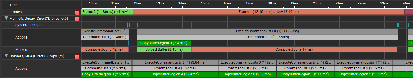
In many cases it’s ideal to use the dedicated COPY queue type to perform this kind of uploading. On NUMA devices this queue typically feeds to a dedicated DMA unit on the video card, which is specifically optimized for performing asynchronous copies of data over the PCIe bus. This not only means it may be more efficient than a copy performed on a DIRECT queue, but it also means that the actual copy operation can potentially run in parallel to other graphics and compute work running on the GPU! For first-time engine initialization this is not a big deal, but for background streaming/loading it’s definitely a better option than forcing your critical per-frame drawing to wait for a bunch of uploads to finish executing (which is what will happen if you submit your copies to your main DIRECT queue). Async copies can still slow down your graphics work a bit by consuming some bandwidth, but this is generally still a better proposition than forcing your graphics work to wait for a bunch of slow PCIe copies to finish. To illustrate the difference, the images below are from two different GPU Trace captures taken with Nvidia Nsight graphics:
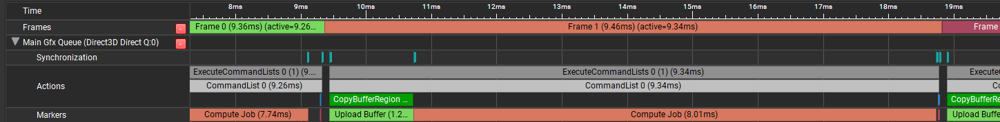

The top image is capture where a 16 MB buffer is uploaded every frame from SysRAM to VRAM using CopyBufferRegion on the main DIRECT queue, which is followed by a compute dispatch that immediately reads from the uploaded buffer. The bottom image shows what things look like if the CopyBufferRegion is instead submitted to a COPY queue, allowing it to overlap with the previous frame’s work on the DIRECT queue. Notice how the frame time is 1.2ms shorter when using the COPY queue, despite the dispatch taking slightly longer when overlapped with the upload.
The trade-off here is that you will take on some significant complexity by using a separate COPY queue instead of re-using your primary queue. Submitting on an async queue means it is now up to you to properly synchronize your submissions across multiple queues: you will need to signal a fence on your COPY queue after submitting a command list and then have another queue wait on that fence before commands on the latter queue can read from the resources being uploaded. This is exactly like “async compute” setups that are common for overlapping compute work with graphics work, and has some of the same headaches. Like async compute, you need to carefully manage the submissions and synchronization between your queues if you’re hoping for them to overlap. You also need to take care not to delete or otherwise re-use your staging buffers until the CPU has fully waited for the COPY fence to be signaled, otherwise you will get incorrect results and/or a GPU crash.
One extra bonus of using a COPY queue is that under the existing (and soon-to-be-legacy) barrier setup there are special rules carved out for resource decay and promotion when a COPY queue is involved. When a resource is copied to or from on a COPY queue, that resource automatically decays back to a COMMON state after the COPY command list finished executing. Since COMMON resources get auto-promoted on their first use, this means that you can typically completely skip issuing any barriers for read-only resources that you initialize this way! This is extremely convenient, and can even save some performance as well.
Before moving on, I should point out that all of the above really only applies for NUMA/dedicated devices. A UMA/integrated device often doesn’t have a dedicated DMA engine, and so any submissions to COPY queues will end up getting serialized/flattened onto a single hardware queue. The typical DEFAULT/UPLOAD setup will still work correctly on ths type of hardware, but if you want to optimize for integrated devices then you may want to consider adding a path that uses custom heaps to allow the CPU to directly initialize your textures.
Two COPY Queues Are Better Than One?
Let’s imagine you’ve setup your engine to be able to submit SysRAM -> VRAM uploads on a COPY queue so that they run asynchronously to your main graphics and compute work that’s performed every frame. You hook this up to the buffer/texture initialization uploads that occur when new resources are created, and it seems to work great. In fact it works so well that you decide to re-use the same path for when the CPU needs to perform per-frame updates of large buffers that live in VRAM. Whenever you peek at a timing capture you see the uploads overlapping with your graphics work, so you consider your work done and move on. But then one day you get reports that the game’s frame time is spiking erratically in areas where there is heavy background streaming, and the spikes appear to be coming from the GPU. You peek at the engine’s timestamp queries surrounding your main graphics queue submission, and confusingly everything looks fine. It’s not until you take a full multi-frame timing capture that you notice the problem:
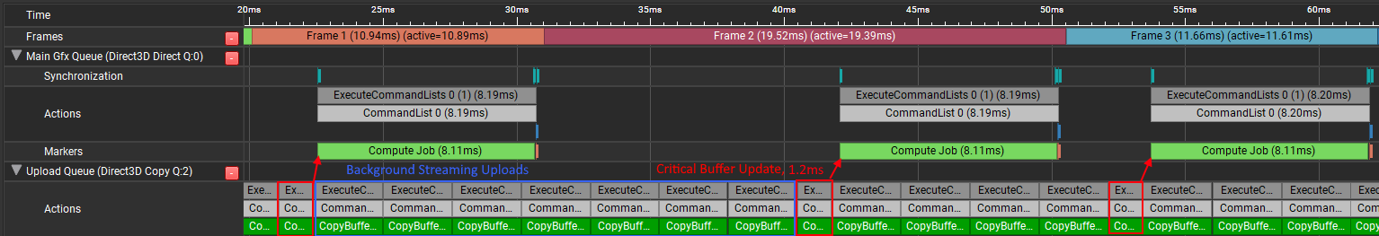
It looks like your uploads from the background streaming are effectively hogging the COPY queue, preventing your more-critical buffer update upload from running. Since your graphics queue waits for the buffer upload to complete, it remains idle for a while which makes the overall frame time longer. This is pretty unfortunate and clearly needs to be fixed, but what should you do? One option is to move your critical upload onto the main DIRECT queue, effectively giving up on getting any overlap for that copy and letting your background uploads have the COPY queue all to themselves:
Things are much improved with this setup. In the fabricated scenario I setup for these captures we’ve gone from a worst-case of 19.39ms down to about 12ms per frame. You’re tempted to submit this and mark the JIRA task as complete, but as a performance-oriented programmer you can’t shake the nagging feeling that we can still do even better than this. It’s just not ideal to require the graphics queue to have to eat the cost of that critical buffer upload, and it’s really not ideal that the critical upload is actually running slower than usual since it’s sharing the PCIe bandwidth with the background uploads (in my test case it’s taking about 2.43ms instead of 1.2ms for a 16 MB buffer, roughly double the time). Seeing how the two submissions end up sharing bandwidth, you think to yourself “wouldn’t it be great if the graphics work, background uploads, and critical uploads could all run asynchronously to each other and the uploads could split the bandwidth?”. Figuring you have nothing to lose, you decide to add a second COPY queue to the engine and redirect all of your critical uploads to that queue instead. Much to your surprise and delight, this works!
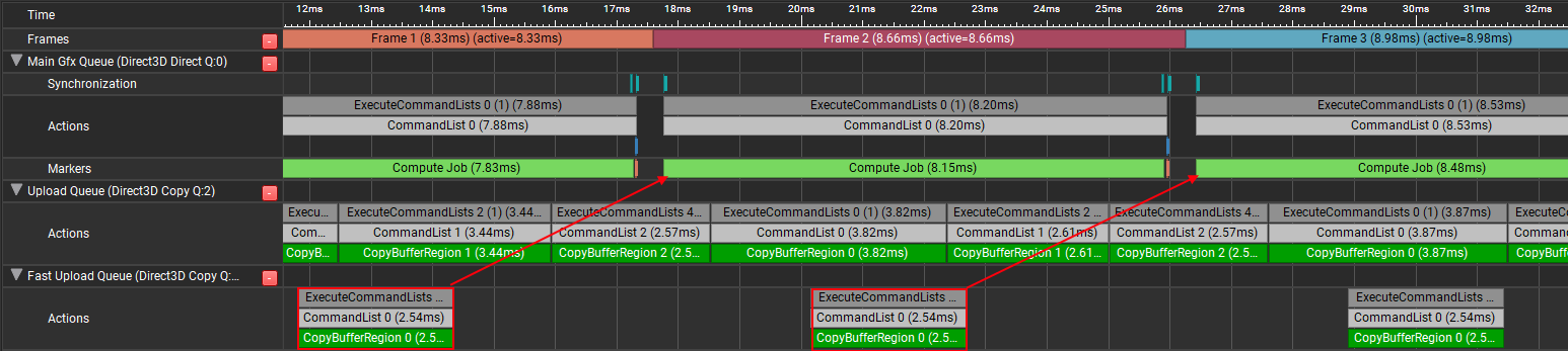
It turns out that dedicated video cards from Nvidia and AMD support this kind of thing, which is advertised by the fact that they expose two transfer queues in Vulkan. What ends up happening is the background uploads and critical upload still share bandwidth which slows down the critical upload, but since the critical upload is able to execute much earlier it doesn’t hold up the main graphics work. This won’t scale up forever: at some point if there are too many critical uploads (or the main graphics work completes too quickly) then the critical upload COPY queue will hold up the main DIRECT/graphics queue. But it’s still absolutely a compelling option for these kinds of advanced scenarios, and likely justifies the additional complexity.
Allocating Staging Memory
As I alluded to earlier, another complicating aspect of the two-step upload is that you need to reserve a sufficient amount of staging memory from somewhere. This memory then needs to remain allocated and untouched until the copying queue completely finishes executing the submission that pulls from the staging buffer. The simple approach seen in some samples is to create a committed buffer resource every time some data needs to be uploaded, and then destroy it after the submission is finished. While this certainly works, creating those committed resoures is definitely not free (especially if you omit the D3D12_HEAP_FLAG_CREATE_NOT_ZEROED flag!), and you could slow down your resource loading and creation by constantly creating and freeing like that. Another tricky issue is memory usage: if you keep allocating more staging buffers, you won’t be able to free them until the GPU consumes them. This can result in unbounded memory usage if many uploads are being batched into a single queue submission during engine initialization. A single big submission with tons of uploads can also be bad on integrated GPUs that don’t have an async DMA unit that you can use, in which case you’re just going to stall the main graphics queue until all of the uploads finish.
As an alternative, one might consider sub-allocating from a single large staging buffer instead of constantly creating new ones. Since the allocation is tied to the GPU progress of copy operations, a ring buffer can be a pretty natural fit. The overall flow could go something like this:
- An upload is requested for N bytes
- Check if there is enough space in the ring buffer, if not stall and wait for previous submissions to finish
- Allocate space in the ring buffer by moving the head back N bytes
- Copy resource data into the ring buffer at the right offset
- Record a copy command on a command list
- Submit the command list on a queue
- Tell the queue to signal a fence once the command list finishes executing
- Periodically check the fence value of previous submissions, if they’ve completed move up the ring buffer tail to free up more space
This is but one possibility for an allocation scheme, and even within such a setup there are more choices to be made. For instance, should it be thread-safe? If multiple threads can use it, which operations can happen in parallel? Is the calling code responsible for copying into the staging buffer and issuing copy commands, or is the uploader mechanism responsible? When should you submit to the GPU, and when should you poll for completed submissions? Should you batch multiple uploads into a single submission? How does this interact with the “main” per-frame submissions on DIRECT and COMPUTE queues? How big should your ring buffer be, and what should happen if an upload exceeds the size of that ring buffer? These questions don’t necessarily have one-size-fits all answer, so it really depends on your engine and use case.
One example of the ring buffer setup can be found in my sample framework. It uses locks to ensure thread-safety by serializing allocations from the ring buffer as well as submissions to the COPY queue, but it allows multiple calling threads to copy into staging memory and record copy commands in parallel once they’ve successfully allocated. It also allows for uploads to happen on background streaming threads that are decoupled from frame rendering. This is achieved by having a 1:1 relationship between uploads and submissions, which is definitely a non-optimal choice for uploading many small resources in succession. In that case the uploads can become bottlenecked by the max number of submissions rather than the ring buffer itself, and overhead from queue submission could start to dominate. The async COPY queue submissions are also waited on by the next frame’s DIRECT/COMPUTE queue submissions, which is always safe (the calling code does not need to wait before using the resource to record commands) but usually too conservative. My framework also pairs this with a FastUploader path that’s intended for “critical” per-frame buffer updates. This path uses its own dedicated COPY queue, and batches all copies from a frame into a single command list and COPY queue submission that’s performed once a frame. It also does not use the staging ring buffer, and instead allows calling code to either aquire some temporary per-frame staging memory or provide its own staging buffer.
As an example of another intriguing approach that makes different trade-offs, consider the uploader that Alex Tardiff wrote for his D3D12Lite framework. Rather than using a ring buffer, the uploader allocates linearly from a staging buffer and fits as many uploads as it can until the staging buffer is exhausted. Every frame the uploads that were staged are submitted in a single command list, and the remaining uploads that do not fit are queued to be uploaded in a subsequent frame. This provides great batching behavior, and effectively enforces a fixed budget in terms of upload bandwidth that will consumed every frame. In comparison to my framework, the main tradeoff is that the uploader handles copying into staging memory and recording D3D12 commands (as opposed to the calling code handling it), which requires the memory containing the source data to be persistent until staging memory frees up. Calling code must also potentially wait several frames until the upload completes, although this kind of synchronization is nicely simplified by tying it to the main frame submission fence. Overall I would say it’s very compelling, and could work well for a lot of scenarios!
For another possible example, check out ResourceUploadBatch from DirectXTK. This helper class still allocates a committed resource for use as staging memory, but allows (manually) batching multiple uploads together into a single submission. It also makes use of std::future as a way of tracking when an upload actually completes, which is a nice touch.
What About DirectStorage?
Some of you may have been asking yourself “hey, how does DirectStorage fit into this?” as you were reading through this section. DirectStorage is capable of fully managing the full journey from disk to staging memory to VRAM all on its own, which is pretty awesome. Unfortunately I’m not personally familar with the inner details of how DirectStorage manages these things, nor do I have much experience with using it. I would assume they are biasing for high throughput of upload operations, since the main goal of that API is to improve loading times. Based on the docs, it sounds like they always suballocate staging memory from a single upload buffer and the operation will fail if the request is larger than the configured staging buffer size. The buffer is then flushed periodically after it fills up to trigger the actual upload to VRAM.
Results From My Testing App
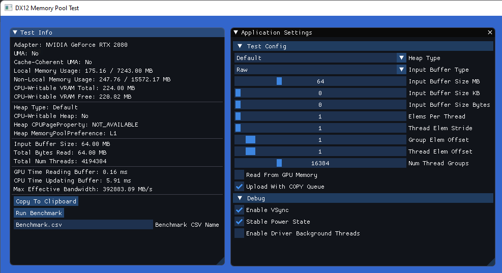
While it’s useful to look at things in terms of theoretical max bandwidth, it’s helpful to gather some actual performance numbers from real working hardware. To that end, I created simple D3D12 application that can and gather timing data from a synthetic performance test. The test itself is nothing fancy: a buffer has its contents updated from the CPU, and then a compute shader is dispatched to read from that buffer. There are options to specify what kind of heap the buffer is allocated from, the size of the buffer, the number of compute shader threads, and the access pattern used by those threads. By timing the CPU update, we can gather some data indicating how quickly or slowly the CPU can fill the buffer with different memory pools and caching protocols. Optionally, we can also time how long it takes to read from the buffer in order to get an idea of how badly this will destroy performance. When the app is run, it presents some real-time results along with a simple interface that looks like this:
In the compute shader itself, a starting address is computed for each thread. The shader then runs an N-iteration loop, where each iteration reads and sums a single 16-byte element of the source buffer. The settings for controlling how the addresses are calculated are a bit obtuse, but together they allow setting up some commonly-seen access patterns to see how they fare with different memory and buffer types. The shader itself is quite short so I’ll post it here for reference:
const uint ThreadGroupSize = 256;

[numthreads(ThreadGroupSize, 1, 1)]
void ComputeJob(in uint3 dispatchThreadID : SV_DispatchThreadID,
                in uint3 groupThreadID : SV_GroupThreadID,
                in uint3 groupID : SV_GroupID)
{
    const uint localThreadIndex = groupThreadID.x;
    const uint globalThreadIndex = dispatchThreadID.x;
    const uint groupIndex = groupID.x;

    #if RawBuffer_
        ByteAddressBuffer inputBuffer = RawBufferTable[AppSettings.InputBufferIdx];
    #elif FormattedBuffer_
        Buffer<float4> inputBuffer = InputBuffers[AppSettings.InputBufferIdx];
    #elif StructuredBuffer_
        StructuredBuffer<float4> inputBuffer = InputBuffers[AppSettings.InputBufferIdx];
    #endif

    float sum = 0.0f;

    // Values with a trailing underscore are compile-time constants, allowing full
    // loop unrolling and dispatch-uniform/wave-uniform buffer access where applicable
    uint elemIdx = (ElemsPerThread_ * ThreadGroupSize * GroupElemOffset_ * groupIndex) +
                    (ElemsPerThread_ * ThreadElemOffset_ * localThreadIndex);
    for(uint i = 0; i < ElemsPerThread_; ++i)
    {
        const uint loadIdx = elemIdx % NumInputBufferElems_;

        #if RawBuffer_
            const float4 data = asfloat(inputBuffer.Load4(loadIdx * 16));
        #elif StructuredBuffer_ || FormattedBuffer_
            const float4 data = inputBuffer[loadIdx];
        #elif ConstantBuffer_
            const float4 data = CBuffer.Elems[loadIdx];
        #endif

        sum += dot(data, 1.0f);

        elemIdx += ThreadElemStride_;
    }

    // Should not actually execute, this is just here to keep the
    // compiler from optimizing away the entire shader
    if(sum < 0.0f)
        OutputBuffer.Store(globalThreadIndex * 4, sum);
}
I’ve used my desktop PC for gathering the data below, which has a Nvidia RTX 2080 with an AMD Ryzen 9 5900X CPU. The GPU has a peak bandwidth of 448 GB/s to VRAM, and as a PCIe 3.0 part it has a max bandwidth of about 16 GB/s for reading memory over that bus. Meanwhile the CPU is connected to 32 GB of DDR4 3600, which has a peak bandwidth of around 28 GB/s per channel, resulting in a total of 56 GB/s for my dual-channel configuration.
CPU Write Performance
Here we’re measuring the time it took for a single 5900X core to fill 16 MB buffer. For this test I only used CPU-accessible memory, since non-CPU-accessible VRAM requires additional work to schedule a GPU copy for the upload. What we see here is that the uncached and cached paths are basically identical, meaning that write combining is doing its job for our simple access pattern we’re using (which is just a memcpy). For the special CPU-accessible VRAM path available through NVAPI, the time grows by about 40% reflecting the fact that we are writing over a slow PCI express bus. For SysRAM this works out to about 15.5 GB/s, while for VRAM it’s about 11.6 GB/s.
CPU Read Performance
For this test case, we want to see how quickly (or slowly) the CPU is able to read from CPU-visible GPU memory. For uncached SysRAM it takes about 4ms to read the entire 16 MB buffer, which is about 4x more time than it took to fill the buffer with write combining. Meanwhile for cached SysRAM it’s about 60x faster, no doubt because the buffer is still present in the cache hierarchy after being filled just prior to the reading step. In real-world scenarios we might expect read performance to be worse for this case since the data may not be present in cache. As for CPU-visible VRAM, we have officially entered “oh no, what I have done?” territory at a whopping 26.66ms. Remember kids: friends don’t let friends read from VRAM on the CPU!
GPU Read Performance, Normal Access
For this test, we are now looking at GPU performance by measuring how long it takes for the GPU to complete the single big compute shader dispatch that reads from the buffer. While this doesn’t serve as a comprehensive bandwidth or cache performance test, it tells us roughly the overall effect that the GPU memory pool will have on GPU performance which is primarily what we are interested in. To gather the data, the test app was configured to use a 64 MB buffer and launch 16 * 1024 * 256 = 4M threads that each access a unique contiguous 16-byte element from the input buffer. This effectively reads from the entire buffer, giving us a rough idea of low long it takes to read the whole thing.
As you would expect for a dedicated GPU, there’s a significant disparity between reading from SysRAM (L0) and VRAM (L1). Reading from SysRAM causes the compute shader to take about ~32x longer to execute relative to VRAM, reflecting the significantly lower theoretical bandwidth for reading over PCIe vs VRAM. This is very close to what we would expect given that my RTX 2080 is rated at 448 GB/s for bandwidth to VRAM, and PCIe 3.0 tops out at 16 GB/s.
To help confirm things, let’s invert these numbers to estimate what the minimum required bandwidth would be in order for the dispatch to complete in the reported time:
While our calculated numbers fall a bit short of the expected theoretical bandwidth, this is probably expected given that our shader may not be hitting the exact conditions required for achieving peak bandwidth on the hardware. However they still clearly reflect the extreme bandwidth deficit that’s experienced when reading from SysRAM.
GPU Read Performance, Non-Coalesced Access
For the previous test, each thread accessed a buffer element that was exactly contiguous with the element being accessed by neighboring threads. GPUs can typically accelerate this case by issuing coalesced memory requests. This pattern is also good in general for cache efficiency: all data from a cache line ends up getting utilized, as opposed to unused neighboring data getting inadvertently pulled into cache. In this test we use a less efficient access pattern where each thread reads a 16 byte element that is 64 bytes away from what their neighboring threads read. If the cache line is 64 bytes, this means that 48 of those 64 bytes are wasted which will slow things down considerably. This is roughly reflected in the test numbers, where the dispatch is about 3-4x slower for all memory types when compared with the previous test case.
GPU Read Performance, Various Buffer Sizes
Earlier in the article we discussed how the size of the buffer being read is something that should factor into our decision of whether to place the buffer in VRAM or SysRAM. The general rule of thumb is “small” buffers are ok being in SysRAM, particularly if they are only read once and/or many threads end up reading the same data from that buffer (constant buffers typically fit this pattern). Let’s try to verify that assumption by running a test where we run a smaller dispatch of 1M threads that access various sizes of smaller buffers. The setup is such that each thread will mod their address with the buffer size, effectively causing the reads to “wrap around”. Therefore if 1M threads each reads a 16-byte element from the input buffer and that buffer is 512 KB, we would expect each byte of that buffer to be read (16 * 1024 * 1024) / (512 * 1024) = 32 times. Let’s now have a look at the results:
At the leftmost end of the chart we see that the gap between SysRAM and VRAM is almost 0 for a tiny 64 KB buffer. This suggests that at typical constant buffer sizes there is little benefit to VRAM, and the speed of the GPU’s cache hierarchies will dominate. As we increase in size though see the SysRAM times pull away from the VRAM times, the latter essentially appearing to have a flat slope at these scales. This suggests that the limited bandwidth of PCIe is bottlenecking the SysRAM dispatch more and more as the buffer size increases, but for VRAM we are likely bottlenecked elsewhere (perhaps on the output writes). Let’s zoom out a bit more and see what we get for 1 to 16 MB buffer sizes:
Up to 4 MB we continue our trend of SysRAM pulling away from the VRAM results, with SysRAM being about 10x slower at that point. But then at 5 MB things jump way up to 1.285 milliseconds, and it stays up there! What gives? What’s so special about 4 MB that things take a nosedive after that point? Well it turns out that 4 MB is the size of the L2 cache on my RTX 2080! Essentially at <= 4 MB the entire buffer was able to fit in L2 cache, which meant that the dispatch time roughly reflected the amount of time it would require to fill that <= 4 MB from memory. If you compute the minimum required bandwidth (buffer size divided by execution time) for these < 4 MB timings, they come out to about 10 GB/s which is fairly close to the 12.5 GB/s I measured from SysRAM in other tests. Meanwhile for the >= 5 MB data, that 1.285 millisecond number that repeats for each test is exactly what you get if you calculate how long it takes to read a 16 MB buffer with 12.5 GB/s bandwidth. 16 MB is what you get if you sum the size of all reads from every thread regardless of the buffer size (1M threads, each reading 16 bytes), which means we’re basically pegged at 12.5 GB/s “effective” bandwidth for these measurements. Since our data set no longer fits comfortably in L2 cache, we can’t count on the data to still be in cache the Nth time an element is accessed by a later thread.
Conclusion
Having to manage separate physical memory pools for GPU programming can be rather complicated, and there are definitely performance pitfalls that we need to watch out for. Integrated GPUs that share a memory pool with the CPU can be simpler, but we still need to interact with them using APIs that accomodate dedicated video cards. In most cases we also need to run the same code on both dedicated and integrated GPUs, which means we need to try to handle both cases gracefully. To minimize the pain, I would recommend the following high-level practices:
- For dedicated video cards:
- Make sure you’re using VRAM for all textures as well as buffers that do not need to be updated from the CPU. The bandwidth difference between SysRAM and VRAM can be nearly 100x on high-end video cards.
- Try to use a COPY/Transfer queue to initialize VRAM resources asynchronously to your graphics work.
- For larger buffers that need to be updated from the CPU, consider allocating them in VRAM and using a staging buffer + COPY/Transfer queue to update them. Consider using two queues if you have both background uploads and critical per-frame uploads.
- On APIs and systems that support it (Vulkan and NVAPI), consider allocating large CPU-updated buffers in CPU-writable VRAM so that you can update them directly. Watch out for potentially slower CPU write performance. Do not read ever from this memory on the CPU!
- For integrated/mobile GPUs:
- Skip using the COPY/transfer queue to initialize or update buffers, you can just make them CPU-writable with no GPU performance penalty.
- With D3D12 you can still use DEFAULT heaps if you like, but it’s still going to be located in SysRAM.
- In general:
- Be careful not to read from memory that is uncached for the CPU, it can be quite slow!
- Try to stick to a simple memcpy when updating GPU memory from the CPU. This will ensure that you play nicely with write combining by writing to the buffer sequentially, and it will also avoid implicit reads that can sometimes occur (for example by summing a value located in GPU memory).
Finally, I’d like to thank the following people for reviewing this post early and providing great feedback:
- Adam Sawicki (extra-special thanks for the suggestion to try using two COPY queues)
- Alex Tardiff
- Jeremy Ong
- Pete Brubaker
- Jiayin Cao
- Brian Collins
That’s all for now, good luck with wrangling those GPUs and their memory pools!
Update 01/04/2024: I’ve uploaded the memory bandwidth testing app to a public GitHub repo in case anybody else would like to try it out. I also updated it to use GPU Upload Heaps from the preview agility SDK, which should be available if you’re running on a system with ReBAR support.
-
D3D12 actually provides two different ways for you to create a texture with a “known” layout that you can encode/decode from the CPU. The first is
D3D12_TEXTURE_LAYOUT_ROW_MAJOR, which uses a standard linear layout that is very inefficient for the GPU to access due to lack of 2D locality. The second is throughD3D12_TEXTURE_LAYOUT_64KB_STANDARD_SWIZZLE, which uses a known standardized swizzle pattern that’s common across hardware. While the standard swizzle sounds like a nice option, in practice Intel/AMD/Nvidia do not actually support it on their hardware. This is likely because the standardized pattern is less efficient than the hardware-specific patterns currently in use. ↩︎